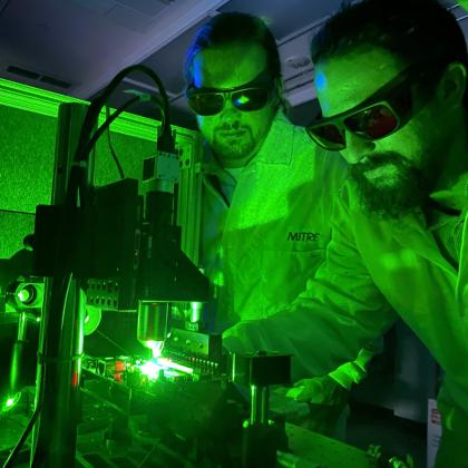
MITRE collaborated with university partners to use the quantum diamond microscope to help identify vulnerabilities in chip technology—both inadvertently and maliciously introduced. The innovation could contribute to microelectronics security for applications in critical infrastructure, transportation, and more.

Using Flaws to Find Flaws: Quantum Sensing for Microelectronics Security
From the components in our smart phones to the integrated circuits in power grids and commercial aircraft, modern microelectronics pervade our way of life. Manufacturing of these tiny chips carries big challenges for global supply-chain stability and security.
Those challenges include a complex semiconductor manufacturing process that can create unintentional defects. Even more concerning: With today’s heavy reliance on overseas fabrication facilities, adversaries could tamper with the supply chain and potentially integrate counterfeit or malicious hardware features, a.k.a. trojans, into devices. Any of those scenarios could damage U.S. national and economic security.

(At left) MITRE's Jacob Lenz and Sean Oliver test a sample on the Quantum Diamond Microscope.
To address this problem, MITRE blended quantum science and semiconductor technology expertise to create a novel tool for microelectronics quality assurance. Researchers within our independent R&D program partnered with experts from Harvard University and the University of Maryland to bring the power of quantum physics to the microelectronics world.
“The quantum diamond microscope [QDM] for microelectronics exploits scientific advancements in quantum research to enable high-precision fingerprinting of chip technology for supply-chain security,” says MITRE physicist Sean Oliver, the project’s principal investigator.
“And we continue to pursue new capabilities that could increase threat-detection efficiency and expand the range to detect future threats.”
Forging the Research to Real-World Connection
Quantum sensing using diamonds—and their flaws—has been around for nearly a decade. The technique uses magnetically sensitive defects purposely embedded within lab-synthesized diamonds to take ultra-precise, highly sensitive measurements of electromagnetic fields. It offers potential for improving capabilities in fields like medical imaging and GPS.
MITRE and our partners added a first-use to the list, with QDM’s application of this powerful technique to characterize microelectronics.
The tool grew out of the academic research, and we were able to bridge the gap between the research problem and our government sponsors’ challenges.
How exactly does it work? The QDM operates much like a regular microscope, but instead of magnifying just the microelectronics chip, the defects in the diamond provide imaging of the circuit’s magnetic field. Because materials that comprise microelectronics do not typically block magnetic fields, the QDM can image functional activity across a wide field of view. This allows testers to non-destructively identify flaws more effectively than traditional tools allow.
Oliver says partnering with academia, along with MITRE’s cross-domain expertise in physics, mathematics, cybersecurity, and microelectronics, drove the project’s success. The patented, award-winning innovation expands on Harvard’s original use case for bioimaging.
“The tool grew out of the academic research, and we were able to bridge the gap between the research problem and our government sponsors’ challenges.”
The research team designed the QDM to function as one of a suite of complementary tools that can assure microelectronics’ quality and security. For example, it could augment the complex process of destructive physical analysis, such as NASA uses for space vehicles. While this destructive testing remains “the gold standard” for quality assurance, our technique could provide a quick means of verification without actually destroying the circuits.
For the near-term goal of helping to secure the microelectronics supply chain, Oliver says expanding collaboration is crucial. “We’re open to opportunities to work with partners from government, academia, and industry to explore the capability’s potential on real devices.”
Join our community of innovators, learners, knowledge-sharers, and risk takers. View our Job Openings.